

— Weller PCB is addressing the growing importance of impedance control in high-speed PCB development, sharing engineering insights into how PCB design parameters, material selection, and manufacturing processes influence signal integrity in advanced electronic systems.
As electronic products adopt faster interfaces and higher data rates, PCB designers face increasing challenges in maintaining stable signal performance. Applications involving Ethernet communication, PCIe-based systems, DDR memory interfaces, industrial networking equipment, and embedded computing platforms require careful management of transmission line characteristics throughout the PCB development process.
Weller PCB has published a detailed PCB Trace Impedance Calculation Guide explaining how trace geometry, dielectric properties, and stackup structures affect impedance performance and high-speed signal behavior.
Controlling Impedance From Design Through Manufacturing
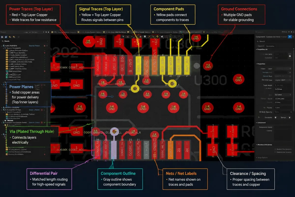
In high-speed PCB applications, signal traces operate as transmission lines rather than simple electrical connections. The electrical characteristics of these transmission lines directly influence signal quality, timing performance, and system reliability.
Key factors affecting PCB impedance include:
- Trace width and copper thickness
- Dielectric thickness between conductive layers
- PCB laminate characteristics
- Layer stackup configuration
- Differential pair spacing and routing geometry
- Manufacturing process tolerances
For example, commonly used controlled impedance designs such as 50Ω single-ended routing and 90Ω differential pairs require close coordination between PCB designers and manufacturers.
A stackup designed for high-speed performance must consider not only theoretical calculations but also real manufacturing conditions. Variations in dielectric thickness, copper etching, and layer registration can affect the final impedance value of a fabricated PCB.
Verification Is an Essential Part of Impedance Control
Achieving target impedance requires more than accurate design calculations. Manufacturing verification plays an important role in confirming that fabricated boards meet electrical requirements.
During PCB production, engineers may use methods such as impedance coupons and TDR (Time Domain Reflectometry) testing to evaluate whether the manufactured PCB matches the specified impedance targets.
This combination of design simulation, manufacturing control, and electrical verification helps reduce signal integrity risks in demanding applications.
Connecting High-Speed Design With Manufacturing Capability
High-speed PCB performance depends on effective coordination between engineering requirements and manufacturing execution.
Through its Printed Circuit Board Assembly Capability, Weller Technology Co. Ltd. supports customers with PCB assembly solutions, manufacturing coordination, engineering communication, and production support for complex electronic applications.
The company works with customers during different stages of product development, including design review, prototype preparation, manufacturing evaluation, and production coordination.
For high-speed electronic products, reliable results require attention not only to PCB layout and impedance requirements but also to the complete manufacturing process.
Helping Engineers Build More Reliable High-Speed Electronics
As PCB designs become smaller and faster, early collaboration between design teams and manufacturing partners becomes increasingly important.
Clear communication about:
- Required impedance values
- PCB stackup structures
- Material selection
- Manufacturing limitations
- Verification methods
allows engineering teams to identify potential risks before production begins.
“A high-speed PCB design is not complete when the impedance value is calculated,” said Kevin Duan of Weller Technology Co. Ltd. “The final performance depends on how well design requirements, manufacturing processes, and verification methods work together.”
Weller PCB continues to provide engineering-focused PCB manufacturing and assembly support for companies developing industrial, communication, and advanced electronic products.
About Weller Technology Co. Ltd.
Weller Technology Co. Ltd. is an engineering-focused PCB manufacturing and electronic manufacturing solutions provider based in Shenzhen, China.
The company works with OEMs, hardware developers, and engineering teams requiring PCB production support, manufacturing communication, and technical collaboration throughout the product development process.
Weller PCB supports customers with PCB fabrication, PCB assembly, engineering review, and production coordination, helping transform complex electronic designs into reliable and manufacturable products.
By combining PCB manufacturing experience with engineering communication, Weller Technology Co. Ltd. focuses on improving manufacturability, production consistency, and product reliability for demanding electronic applications.
Media Contact
Kevin Duan
Weller Technology Co. Ltd.
Email: kevinedard.dw@gmail.com
Address: 4/F, Bldg.3, Huafeng Longgang Overseas Returnees Ind. Park,
Baolong 1st Rd, Nanyue Community, Baolong Street,
Longgang District, Shenzhen, Guangdong, China
Postal Code: 518116
Website – https://wellerpcb.com/
LinkedIn: Weller PCB
https://www.linkedin.com/company/wellerpcbs/
Contact Info:
Name: Kevin Duan
Email: Send Email
Organization: Weller Technology Co. Ltd.
Website: https://wellerpcb.com/
Release ID: 89201754
If you detect any issues, problems, or errors in this press release content, kindly contact error@releasecontact.com to notify us (it is important to note that this email is the authorized channel for such matters, sending multiple emails to multiple addresses does not necessarily help expedite your request). We will respond and rectify the situation in the next 8 hours.